


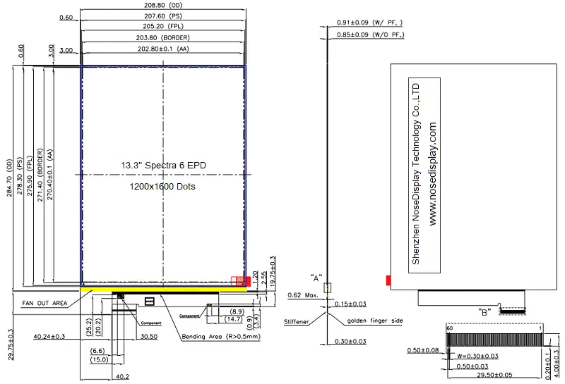
Mechanical Drawing & Interface Definition
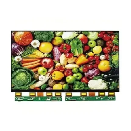
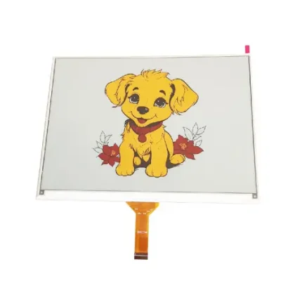
Model: ND133EPN16001200-A01
Download Center Contact an Engineer
PIN Description
| Pin No. | Symbol | Description |
|---|---|---|
| 01 | VCOMBD_M | VCOMBD driving voltage (Master). (I/O: P) |
| 02 | RESEC | Current sense input pin for the control loop. (VCOM) (I/O: I) |
| 03 | GDRC | N-Channel MOSFET gate drive control. (VCOM) (I/O: O) |
| 04 | RESEN | Current sense input pin for the control loop. (VDDN) (I/O: I) |
| 05 | GDRN | P-Channel MOSFET gate drive control pin. (VDDN) (I/O: O) |
| 06 | RESEP | Current sense input pin for the control loop. (VDDP) (I/O: I) |
| 07 | GDRP | N-Channel MOSFET gate drive control pin. (VDDP) (I/O: O) |
| 08 | GND | Ground. (I/O: P) |
| 09 | AVDD | Analog voltage supply. (DC/DC) (I/O: P) |
| 10 | VDD | Analog/digital voltage supply. (I/O: P) |
| 11 | NC | No connection and do not connect with other NC pins. (I/O: —) |
| 12 | VCC | LDO output pin. (I/O: P) |
| 13 | VDDP | Positive power supply for analog circuit. (+16V ~ +19V) (I/O: P) |
| 14 | VDDP | Positive power supply for analog circuit. (+16V ~ +19V) (I/O: P) |
| 15 | NC | No connection and do not connect with other NC pins. (I/O: —) |
| 16 | VDDN | Negative power supply for analog circuit. (−19V ~ −16V) (I/O: P) |
| 17 | VDDN | Negative power supply for analog circuit. (−19V ~ −16V) (I/O: P) |
| 18 | VCC1 | Positive power supply only for oscillator. (I/O: P) |
| 19 | VDDIO | Power input for IO. (I/O: P) |
| 20 | TSCL | I2C interface to digital temperature sensor clock pin. (I/O: I/O) |
| 21 | TSDA | I2C interface to digital temperature sensor data pin. (I/O: I/O) |
| 22 | BS0 | Input interface setting. Select 3-wire / 4-wire / Quad SPI interface. (Default: H) (I/O: I) |
| 23 | BS1 | Input interface setting. Select 3-wire / 4-wire / Quad SPI interface. (Default: H) (I/O: I) |
| 24 | RES# | Reset. (I/O: I) |
| 25 | BUSY_N | This pin indicates the driver status. Connect with a pull-up resistor to VDDIO. BUSY_N = “0”: Driver is busy, data/VCOM is transforming. BUSY_N = “1”: Non-busy. Host side can send command/data to driver. (I/O: O) |
| 26 | D/C# | Command/Data input. L: command; H: data. (4-wire SPI). Connect to GND in 3-wire mode or standard 4-wire mode. (I/O: I) |
| 27 | CSB_M | Serial communication chip select. (Master) (I/O: I) |
| 28 | SCL | Serial communication clock input. (I/O: I) |
| 29 | SI0 | Serial communication data input/output (3-wire/4-wire SPI). Serial communication data input (Standard 4-wire SPI). (I/O: I/O) |
| 30 | SI1 | Serial communication data input. Serial communication data output. (Standard 4-wire SPI). (I/O: I/O) |
| 31 | SI2 | Serial communication data input. (Standard 4-wire SPI Quad mode) (I/O: I) |
| 32 | SI3 | Serial communication data input. (Standard 4-wire SPI Quad mode) (I/O: I) |
| 33 | DRVP_Gate | Driving external N-MOSFET (VGP). (I/O: O) |
| 34 | FBP | Positive charge pump (VGP) feedback pin. (I/O: I) |
| 35 | GND | Ground. (I/O: P) |
| 36 | VCOMBD_S | VCOMBD driving voltage (Slave). (I/O: O) |
| 37 | DRVN | Driving external BTJ. (VGN) (I/O: O) |
| 38 | FBN | Negative charge pump feedback pin. (VGN) (I/O: I) |
| 39 | REG_VGN | VGN internal reference voltage output. (I/O: O) |
| 40 | DRVN2 | Driving external BTJ. (VNCP_3P5V) (I/O: O) |
| 41 | VNCP_3P5V | Negative power supply for analog bias1 circuit. (for TFT_Vcom) −3.5V deviation ±4.5%. (I/O: P) |
| 42 | VSPH | Positive source buffer output. (I/O: P) |
| 43 | VSPL | Positive source buffer output. (I/O: P) |
| 44 | VSPL2 | Positive source buffer output. (I/O: P) |
| 45 | VSPHI | Positive source voltage. (I/O: P) |
| 46 | VSPLI | Positive source voltage. (I/O: P) |
| 47 | VSPL2I | Positive source voltage. (I/O: P) |
| 48 | VSNH | Negative source buffer output. (I/O: P) |
| 49 | VSNL | Negative source buffer output. (I/O: P) |
| 50 | VSNL2 | Negative source buffer output. (I/O: P) |
| 51 | VSNL2I | Negative source voltage. (I/O: P) |
| 52 | VSNLI | Negative source voltage. (I/O: P) |
| 53 | VSNHI | Negative source voltage. (I/O: P) |
| 54 | FPL_VCOM | FPL_VCOM driving voltage. (I/O: O) |
| 55 | TFT_VCOM | TFT_VCOM driving voltage. (I/O: O) |
| 56 | VBB_3P5V | Negative power supply for analog bias2 circuit. (for TFT_Vcom) −3.5V deviation ±4.5%. (I/O: P) |
| 57 | NC | No connection and do not connect with other NC pins. (I/O: —) |
| 58 | CSB_S | Serial communication chip select. (Slave) (I/O: I) |
| 59 | VGH | Positive Gate driving voltage. (I/O: P) |
| 60 | VGL | Negative Gate driving voltage. (I/O: P) |
Sample Ordering & Delivery
Evaluate ND133EPN16001200-A01 13.3-inch engineering samples before integration. Shipping is charged separately; import duties and taxes are excluded. Estimated delivery includes preparation. Confirm final terms before payment.
Sample MOQ
2 pcs per modelMinimum 2 pcs per model.
Preparation Time
4 daysAfter order and payment confirmation.
Standard Delivery
Shipping Fee
Transit Time: ~11 days
Total Time: ~15 days
Express Delivery
Shipping Fee
Transit Time: ~4 days
Total Time: ~8 days


Quality & Compliance Support
We provide quality and compliance documentation for qualified OEM projects
based on the selected module, BOM and manufacturing configuration.
RoHS
EU RoHS compliant materials and process control
REACH
Support REACH regulation compliance
Reliability Testing
Environmental & mechanical reliability testing reports
ESD Control
ESD protection design and testing capability
Quality System
Manufactured under a certified quality management system
Documentation availability and scope are confirmed according to the selected module, BOM, manufacturing source and project requirements.